Main Menu

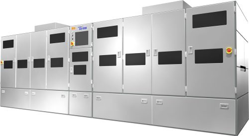
Full-Automatic Direct lmaging System with UV Light Source

PLAY VIDEO:
EDi-5308
Best match for IC package SR exposure
EDi-8308 EDi-8310
High-speed SR lmaging for HDl panels
Field-proven UV Direct Imaging System
De-facto Standard for Solder Resist lmaging
Features
- New model with finer resolution and higher speed capability added to
EDi family; an industrial standard for IC substrate solder mask exposure.
It can be equipped with automatic wavelength cut filter swiching function. (EDi-5308 Option) - Latest photovia material can be imaged, suitable for micro via which is
difficult to process by laser drill machine. - New concept high aliment accuracy function for FO-PLP die shift issue
(Die by Die Alignment Option) - Enlarging HDI panel imaging (EDi-8310)

